


| Location:Home > HDI PCB > 6-layer 2nd-order HDI PCB |
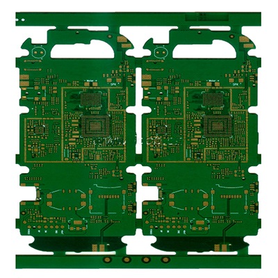
6-layer 2nd-order HDI PCBProduct type:6-layer 2nd-order HDI PCBMaterial:FR4 联茂 Layers/plate thickness:6-layer/0.8mm Surface treatment:Shen Jin+OSP Line width/line spacing:2.5mil/2.5mil Applications:communication Contact Us |
The two-stage HDI board has a staggered hole structure and a laminated structure. The so-called staggered hole means that the two layers of laser holes are staggered. Why stagger it? Because the copper plating is not satisfied, the inside of the hole is empty, so it is not possible to directly drill the hole on it.
6 layers of second-order = 4 layers of first-order plus 2 layers. 8 layers of second-order = 6 layers of first-order plus 2 layers.

Stacked orifice plate, the process is complicated and the price is higher. The two layers of laser holes of the staggered hole board are overlapped, and the circuit will be more compact. The inner layer laser hole needs to be plated and filled, and then the outer layer laser hole is made. The price is more expensive than the wrong hole.


