


| Location:Home > IC Substrate > LGA package carrier board |
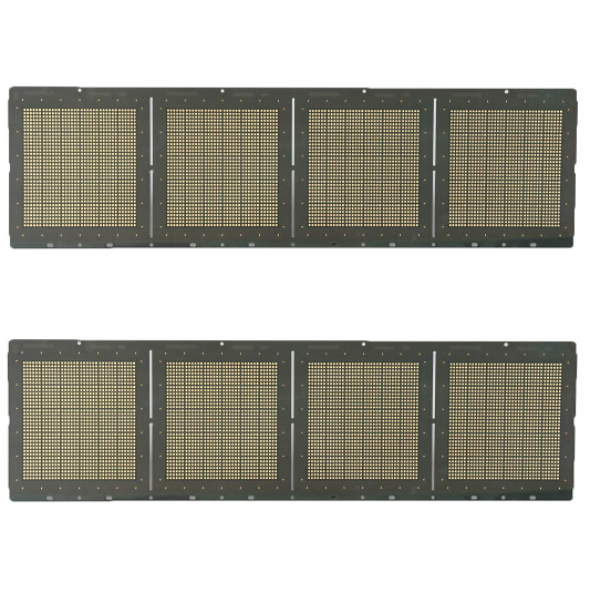
LGA package carrier boardProduct type:LGA package carrier boardMaterial:HL832NXA Layers/plate thickness:2-layer/0.2mm Surface treatment:Nickel Palladium Gold Line width/line spacing:75um-25um Applications:IC carrier board, IC substrate Contact Us |
Description:
LGA package carrier board features
High Density Junction Structure
Via Fill Plating and Stacked Via Structures
Various surface treatments
High requirements for sheet and surface flatness
LGA package carrier board using process
Semi-additive method, laser drilling
LGA package carrier board application
Smartphones, Computers, IoT Products, Messaging Electronics


