


| Location:Home > Buried Blind Vias PCB > 16-layer photovoltaic backplane |
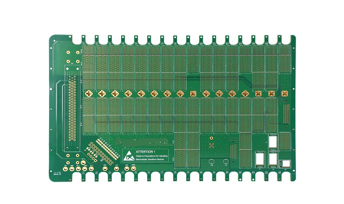
16-layer photovoltaic backplaneProduct type:16-layer photovoltaic backplaneMaterial:FR4 Layers/plate thickness:16-layer/2.4mm Surface treatment:Immersion Gold Line width/line spacing:4mil/4mil Applications:IC electronic assembly Contact Us |
A backplane PCB, also known as a motherboard pcb, is a substrate that carries functional pcbs, including child pcbs or line cards. The main task of the backplane is to carry the sub-pcbs and distribute power to the functional pcbs for electrical connection and signal transmission. Therefore, the system function can be obtained through the cooperation of the backplane and its sub-pcbs.
With the improvement of the integrity of electronic (IC) components and the increase in the number of I/Os and the rapid development of electronic technology assembly, after high-frequency signal transmission and high-speed digitization, the function of the backplane gradually covers the carrying, signal transmission and distribute. To achieve these functions, backplanes must meet higher requirements, including layer count (20 to 60 layers), board thickness (4mm to 12mm), number of vias (30,000 to 100,000), reliability, frequency, and signal transmission.
Our company specializes in PCB manufacturing and has many years of rich experience in PCB manufacturing. We are committed to providing global customers with fast and high-quality PCB boards at reasonable prices. Each circuit board is produced in accordance with strict standards and meets IPC, RoHS and other standards. Ensure that the PCB circuit board meets customer requirements.


